Subscribe
18:00Tao calls OpenAI’s Navier–Stokes push “resource extraction”17:10LAPTOP memecoin hits $190.81, then loses 99% inside an hour17:05Hubinger puts the odds of AI killing everyone above 10%; a colleague resigns16:39CancerBench launches; five frontier models tied at zero cancer types cured16:30ElevenLabs preparing 2028 IPO after $11bn round, The Information reports16:30Anthropic retracts its July explanation: Mythos 5 attacked systems knowingly
Hardware2 min read

LG Innotek showed a package substrate bigger than eleven reticle-limited dies

The first FC-BGA it has built for AI accelerators runs past 100mm on a side, with mass production targeted for 2027 and glass cores for 2028.
In briefLG Innotek unveiled its first FC-BGA for AI accelerators at KPCA Show 2026 in Incheon Songdo, a large-area substrate over 100mm on a side, with mass production targeted for 20271LG Innotek will also show an 85mm large-area FC-BGA and an ultra-large-area sample about 40% greater in area2The new AI accelerator FC-BGA is about six times the size of a PC FC-BGA sample3
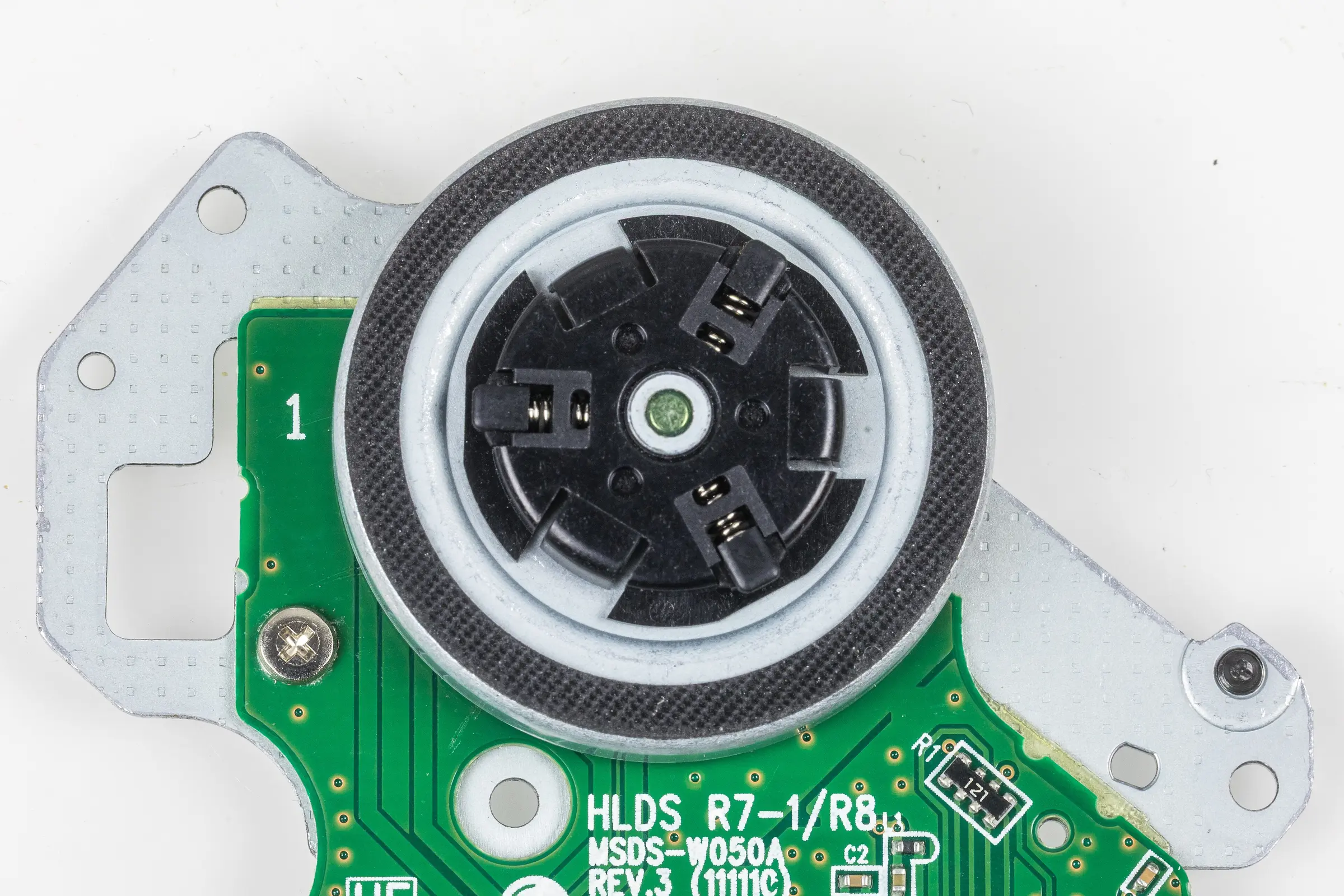
An LG Innotek printed circuit board
Photo: Raimond Spekking (CC BY-SA 4.0)

LG Innotek showed its first FC-BGA built for AI accelerators at the KPCA Show in Incheon on September 9th: a substrate more than 100mm on a side, which the company says is about six times the area of the PC substrate it sat next to. Mass production is targeted for 2027.

The chip is not the thing that limits how big an AI package can get. The board underneath it is.

Package and die area (mm²)
Largest single die at the EUV reticle limit858PC FC-BGA implied by LG Innotek's own comparison1,667LG Innotek 85mm large-area FC-BGA7,225New AI accelerator FC-BGA at 100mm per side10,000

Run the arithmetic on the release and it becomes clearer than the copy. An 85mm square is 7,225mm². A 100mm square is 10,000mm², which is 38% more — and the release separately advertises an "ultra-large-area" sample about 40% bigger than the 85mm part. Those are the same board. Against a maximum single die at the 26×33mm reticle limit, the new substrate is close to twelve times the area, which is the point: this is a carrier for a package of many dies and stacks of memory, not for a chip.

Two other things at the booth matter more than the size.

Chip embedding puts silicon inside the substrate rather than on top of it, which shortens the connection and cuts resistive loss. And glass, which LG Innotek is targeting for mass production in 2028, replaces the core layer to hold the board flat. Warpage is the reason large-area organic substrates are hard. A big ABF board bends as it heats, circuits distort, and yield falls. So the 2028 date is arguably the more important one on this stand, because flatness is what makes area usable.

The quieter number is Cu-Post, which stands copper pillars on the substrate and puts the solder ball on top of them. LG Innotek says this cuts the spacing between solder balls to roughly a fifth of what it was, and that copper conducts heat more than seven times better than the lead it replaces. More I/O, cooler package, same footprint.

Now, is any of this a business yet?

LG Innotek's package solutions division did 935.6bn won of revenue and 99.6bn won of operating profit in the first half of 2026, with margin up from 6.5% to 10.6% and operating profit nearly doubling year on year. The company's stated goal is a trillion won of operating profit from this business by 2031. Annualise the half and you get about 199bn won — so the target asks for roughly five times the current run rate in five years, which is a long way to travel on a substrate that has not been qualified by a named customer.

Because that is the fair objection here. A sample at a trade show is not a design win, and the high end of this market belongs to incumbents. On the Taiwanese side, Unimicron's advanced substrates already sit inside TSMC's 3DFabric alliance (next to CoWoS and SoIC, which is the seat everyone wants). Nobody at LG Innotek claimed an accelerator customer this week.

We would expect one to be named before the end of 2027, or the 2027 production date to move. Watch which of those happens first — and if you follow the packaging supply chain, watch the glass date harder than the area.

Sources

01
LG Innotek unveiled its first FC-BGA for AI accelerators at KPCA Show 2026 in Incheon Songdo, a large-area substrate over 100mm on a side, with mass production targeted for 2027이번 전시에서 LG이노텍은 AI 가속기용 FC-BGA를 처음으로 공개한다. ... 이번에 공개되는 AI 가속기용 FC-BGA는 한 변의 길이가 100mm를 넘는 대면적 기판이다. ... 회사는 AI 가속기를 포함한 AI 학습 및 추론용 고부가 FC-BGA를 2027년 양산한다는 목표다.” — lginnotek.com · primary · Sep 10
02
LG Innotek will also show an 85mm large-area FC-BGA and an ultra-large-area sample about 40% greater in area또한 LG이노텍은 전시 기간 동안 가로∙세로 85mm FC-BGA 대면적 기판뿐 아니라, 이보다 면적이 약 40% 늘어난 초대면적 FC-BGA 기판 샘플도 선보일 계획이다.” — lginnotek.com · primary · Sep 10
03
The new AI accelerator FC-BGA is about six times the size of a PC FC-BGA sample[사진2] LG이노텍이 KPCA show 2026에서 첫 선보인 대면적 ‘AI 가속기용 FC-BGA’(오른쪽), PC용 FC-BGA 샘플(왼쪽) 대비 약 6배가량 크다.” — lginnotek.com · primary · Sep 10
Show all 11 sources
04
LG Innotek's chip embedding places the chip inside the substrate to shorten connections and reduce power loss칩 임베딩(Chip Embedding) 기술이 대표적이다. 기판 표면에 칩을 실장하는 기존 방식과 달리, 기판 내부에 칩을 넣어 칩과 기판 간 연결 거리를 최소화한 기술이다. 신호 전달 성능을 높이면서도 전기 저항을 낮춰 전력 손실을 줄일 수 있다.” — lginnotek.com · primary · Sep 10
05
LG Innotek's glass substrate replaces the core layer with glass to minimise warpage and circuit distortion, with mass production targeted for 2028유리기판은 기판 내부 코어(Core)층을 유리로 대체해, 기판의 휨 현상과 회로 왜곡을 최소화할 수 있다는 장점이 있다. LG이노텍은 2028년 유리기판 양산을 목표로 기술 개발에 속도를 내고 있다.” — lginnotek.com · primary · Sep 10
06
LG Innotek's Cu-Post method reduces solder ball spacing to about 20% of the previous level and uses copper with more than seven times the thermal conductivity of lead이 기술은 반도체 기판에 초미세 구리 기둥을 세우고, 그 위에 납땜용 구슬인 솔더볼(Solder Ball)을 얹어 기판과 메인보드를 연결하는 방식이다. 기존 대비 솔더볼 간격을 약 20% 수준까지 줄여 더 많은 회로를 배치할 수 있다. 납 대비 열전도율이 7배 이상 높은 구리를 활용하여 발열을 개선한 것도 주요 강점이다.” — lginnotek.com · primary · Sep 10
07
LG Innotek's package solutions business posted 935.6bn won of revenue and 99.6bn won of operating profit in the first half of 2026, up 18% and 94%, with margin rising from 6.5% to 10.6%, and targets 1 trillion won of operating profit by 2031한편 LG이노텍 패키지솔루션사업은 올 상반기 매출 9356억원, 영업이익 996억원으로, 전년 대비 각각 18%, 94% 증가했다. 영업이익률 역시 6.5%에서 10.6%로 상승하며 성장성과 수익성을 모두 입증했다. LG이노텍은 패키지솔루션사업을 미래 핵심 성장축으로 삼고 2031년까지 영업이익 1조원 규모로 육성하겠다는 방침이다.” — lginnotek.com · primary · Sep 10
08
KPCA Show 2026 runs from September 9 to 11 at Songdo Convensia in Incheon with more than 350 exhibitors오는 9일부터 11일까지 인천 송도 컨벤시아에서 열리는 ‘KPCA show 2026(국제 반도체 기판 및 첨단 패키징 산업전)’에 참가, 차세대 기판 기술 및 제품을 선보인다. ... 국내외 350여개 업체가 참가해, 최신 기술 동향을 공유한다.” — lginnotek.com · primary · Sep 10
09
harukaze5719 reported the LG Innotek FC-BGA unveiling on September 9, 2026LG Innotek has unveiled FC-BGA. The revealed product is a large-area substrate with a side length exceeding 100mm, with a target of mass production in 2027.” — x.com · reported · Sep 10
10
A conventional EUV exposure field of 26x33mm bounds a single die at about 858 square millimetresConventional 0.33-NA EUV has 4X magnification in both directions, enabling the familiar 26×33 mm exposure field with traditional 6-inch photomasks.” — tomshardware.com · reported · Sep 10
11
Unimicron's high-end substrates are part of TSMC's 3DFabric alliance alongside Alchip, ASE and SPIL供應鏈創意、世芯-KY的客製化晶片設計服務,日月光、矽品封裝測試,以及欣興的高階載板,均已納入台積電3DFabric聯盟分工。” — ctee.com.tw · reported · Sep 10
Up next · Keep readingHardware · 3 min read

A20 Pro is the first 2nm phone chip. The number that matters is 32 Neural Engine cores after three years at 16

Apple doubled the Neural Engine, widened memory bandwidth 50 percent, moved the DRAM off the thermal path and tripled the vapor chamber. Every one of those decisions is about running models on the phone.

Continue ↓